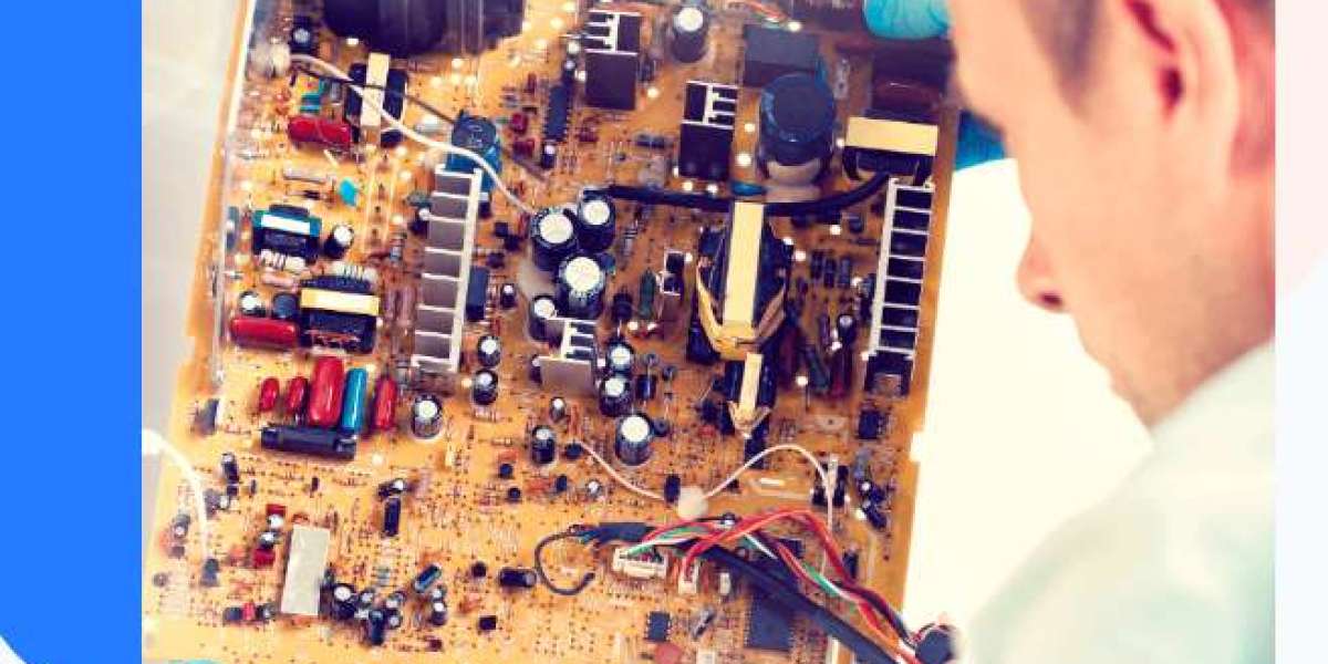

Modern electronic products rely on printed circuit boards (PCBs) to connect and support the components that power everything from industrial equipment and medical devices to robotics and consumer electronics. While a schematic defines how a circuit should function, the physical layout of the PCB determines how efficiently and reliably it performs. This is why professional PCB layout services are essential for creating products that meet demanding performance, manufacturing, and reliability standards.
Wagner Engineering provides PCB layout services focused on transforming electronic concepts into production-ready circuit boards. By combining engineering expertise with careful attention to signal integrity, power distribution, thermal management, and manufacturability, the company develops PCB layouts that balance technical performance with practical manufacturing requirements.
What Are PCB Layout Services?
PCB layout services involve converting an approved electronic schematic into a physical circuit board design that can be manufactured and assembled. This process includes component placement, trace routing, layer stack-up design, power and ground plane optimization, design rule verification, and preparation of manufacturing files.
An effective PCB layout ensures that electrical signals travel efficiently, heat is properly managed, electromagnetic interference (EMI) is minimized, and the final board can be manufactured with fewer defects. Every design decision directly impacts product reliability, performance, and production costs.
Why PCB Layout Matters
Even the best electronic circuit can experience performance problems if the PCB layout is poorly designed. Improper routing, inadequate grounding, or poor component placement may introduce signal noise, thermal issues, and manufacturing challenges.
Professional PCB layout services help deliver several important benefits:
Improved signal integrity
Reliable power distribution
Better thermal performance
Reduced electromagnetic interference (EMI)
Easier manufacturing and assembly
Simplified debugging and maintenance
Higher long-term product reliability
A carefully engineered layout minimizes costly design revisions while supporting faster product development and production.
Wagner Engineering's PCB Layout Expertise
At Wagner Engineering, PCB layout is treated as both an engineering discipline and a precision design process. Their engineers use advanced design techniques to optimize every aspect of the circuit board, from component placement to multilayer routing.
The company focuses on creating layouts that are functional, visually organized, and optimized for manufacturing. Their engineering team carefully considers signal integrity, high-speed circuit requirements, RF applications, power delivery, and thermal management to produce dependable PCB designs for complex electronic systems.
Comprehensive PCB Layout Process
Professional PCB layout follows a structured workflow that ensures every design meets technical and manufacturing requirements.
Design Review
The process begins with reviewing the electrical schematic, component selection, mechanical constraints, and project specifications. This step ensures the layout strategy aligns with product objectives.
Component Placement
Strategic placement of components is one of the most critical aspects of PCB layout. Engineers position components to optimize electrical performance, simplify routing, improve heat dissipation, and reduce interference.
Trace Routing
Conductive traces are routed carefully to maintain signal quality while minimizing crosstalk, impedance mismatches, and noise. Proper routing also supports reliable communication between components and improves overall system performance.
Power and Ground Optimization
Well-designed power and ground planes provide stable voltage distribution while reducing electrical noise. Proper grounding improves system reliability and electromagnetic compatibility.
Design Verification
Before manufacturing, the PCB undergoes extensive verification, including design rule checks (DRC), clearance analysis, manufacturability reviews, and electrical validation to identify potential issues early in the development process.
Supporting Advanced PCB Technologies
Today's electronic products often require more sophisticated PCB layouts than ever before. Wagner Engineering develops layouts for a variety of advanced applications, including:
Multilayer circuit boards
High-speed digital systems
RF and wireless electronics
Embedded systems
Industrial automation
Medical devices
Robotics
IoT products
Their multidisciplinary engineering experience enables them to create PCB layouts that meet demanding technical specifications while remaining practical for manufacturing and assembly.
Benefits of Professional PCB Layout Services
Working with an experienced PCB layout provider offers significant advantages throughout the product development lifecycle.
Key benefits include:
Reduced development time
Improved manufacturing yields
Lower production costs
Enhanced product performance
Greater system reliability
Easier product maintenance
Better scalability for future revisions
By addressing electrical and manufacturing challenges during the layout stage, businesses can avoid expensive redesigns later in production.
Design for Manufacturability (DFM)
An effective PCB layout must not only perform well electrically but also be easy to manufacture consistently. Wagner Engineering incorporates Design for Manufacturability (DFM) principles throughout the layout process to reduce fabrication complexity and improve production efficiency.
Optimized trace widths, appropriate spacing, accessible test points, and logical component placement help simplify assembly while minimizing manufacturing defects. These practices contribute to shorter production cycles and more reliable finished products.
Why Choose Wagner Engineering?
Selecting the right engineering partner is essential for successful PCB development. Wagner Engineering combines expertise in PCB design, embedded systems, firmware, software development, and cloud technologies to provide comprehensive engineering solutions.
Clients benefit from:
Customized engineering services
Experienced multidisciplinary engineers
Precision PCB layouts
Focus on quality and reliability
Collaborative project management
Long-term technical support
The company works closely with clients throughout the design process, ensuring each PCB layout meets both technical requirements and business objectives. Their commitment to engineering excellence helps organizations accelerate product development while maintaining high standards of quality.
High-quality PCB layout services form the foundation of reliable electronic products. From component placement and signal routing to thermal optimization and manufacturability, every aspect of the layout influences product performance and long-term reliability.
Whether you're developing an IoT device, industrial controller, medical system, robotics platform, or next-generation consumer electronics, partnering with an experienced engineering firm like Wagner Engineering provides the expertise needed to transform your design into a production-ready PCB. Through precision engineering, collaborative development, and a strong focus on quality, Wagner Engineering helps businesses bring innovative electronic products to market with confidence.